HVDC Thyristor Valves
Inside every HVDC converter station — whether it is rectifying AC to DC at a hydroelectric dam in Sichuan or inverting it back to AC at a load centre in Shanghai — there is a valve hall. And inside that hall, rising in insulated columns several metres tall, are the thyristor valves. They carry no moving parts. They make no sound. Yet they switch currents of thousands of amperes and withstand voltages of hundreds of kilovolts, doing so millions of times a year with a reliability that underpins continental power supply. Understanding what a thyristor valve is, how it differs from the thyristor device itself, and how these assemblies are fired, housed, and tested is essential to understanding how HVDC transmission actually works.
The Thyristor Device: A Silicon Switch at the Atomic Scale
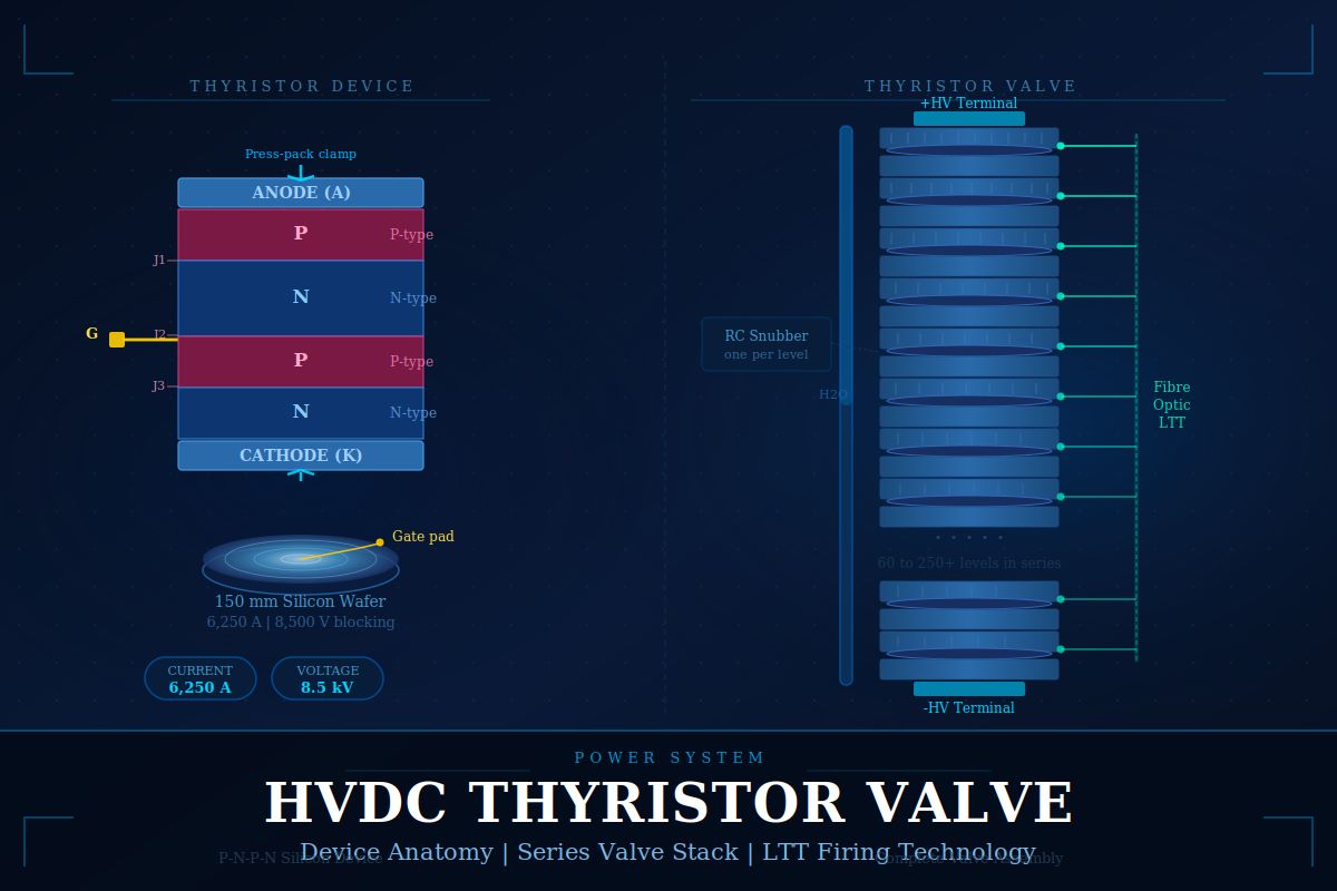
A thyristor — also called a Silicon Controlled Rectifier (SCR) — is a four-layer, three-junction semiconductor device with the structure P-N-P-N. It has three terminals: the Anode (A), the Cathode (K), and the Gate (G). In its off state, the device blocks voltage in both forward and reverse directions. When a brief current pulse is applied to the Gate while the anode is positive with respect to the cathode, the device fires — it conducts heavily and continues to do so until the anode current naturally falls below a holding current threshold. This self-latching behaviour is the defining characteristic of the thyristor and what makes it ideally suited to line-commutated converter (LCC) HVDC systems, where the AC network itself provides the voltage reversal that extinguishes conduction.
For HVDC service, thyristors are not ordinary SCRs scaled up. They are highly engineered devices manufactured from large-diameter silicon wafers — typically 100 mm to 150 mm in diameter — diffused with precisely controlled dopant profiles. A single HVDC thyristor disc can handle a continuous on-state current of 3,000 to 6,250 amperes (RMS) and must block forward and reverse voltages of 6,000 to 8,500 volts in the off state. The silicon wafer is housed between two high-conductivity copper or molybdenum pressure contact electrodes, which simultaneously provide electrical contact and thermal conduction to the cooling system.
The P-N-P-N Latch: The four-layer thyristor can be modelled as two interconnected bipolar transistors — a PNP and an NPN — with their bases and collectors cross-coupled. Once the gate pulse triggers the NPN transistor into conduction, the resulting collector current drives the base of the PNP transistor, which in turn sustains the NPN — creating a regenerative latch. The device remains latched on until the anode-cathode current drops to zero, which in an AC system occurs naturally at every current zero crossing.
The Thyristor Valve: Device vs. Assembly
The distinction between a thyristor device and a thyristor valve is fundamental and is often confused in general engineering literature. A thyristor device is the individual semiconductor disc — the silicon wafer in its enclosure. A thyristor valve is the complete engineered assembly of many such devices connected in series, together with all associated electrical, thermal, mechanical, and control components, that together perform one switching function in the converter circuit.
Because a single thyristor disc can block only 6–8.5 kV, hundreds must be stacked in series to achieve the valve voltage rating demanded by a ±500 kV or ±800 kV HVDC system. A valve for a ±500 kV LCC-HVDC project typically contains 60 to 100 thyristor levels in series. At ±800 kV, this may rise to 150 or more levels. Each level in the series stack consists of one or two thyristor discs (for redundancy) clamped mechanically between heat sinks, which are themselves connected in a cooling circuit. A voltage-dividing snubber circuit — typically a resistor-capacitor (RC) network — is fitted at each level to ensure that voltage is distributed uniformly across all devices during transient switching events.
Firing Technology: How Thyristors Are Triggered in a Valve
Triggering a thyristor in a low-voltage laboratory circuit is straightforward — a small current pulse to the gate suffices. Triggering hundreds of thyristors stacked at potentials of several hundred kilovolts above earth, simultaneously and reliably, is one of the core engineering challenges of HVDC valve design. Two approaches have evolved and coexist in modern installations.
In Electrically Triggered Thyristor (ETT) systems, the firing pulse originates from ground-potential control electronics and is transmitted up the valve column via a chain of pulse-transformer-coupled gate drive circuits — one per thyristor level. Each level draws its firing energy from the voltage across itself, requiring a minimum charge-up time before a firing command can be issued. ETT technology is well-established and economical, but introduces complexity in the inter-level isolation circuitry. Failures in the firing chain can cascade if not correctly detected.
In Light-Triggered Thyristor (LTT) systems, a fibre-optic cable delivers a pulse of light directly to each thyristor’s gate, which incorporates an integrated photodiode and gate amplifier structure within the silicon itself. The control system at earth potential transmits firing commands as optical pulses — one fibre per thyristor level — providing complete galvanic isolation without pulse transformers. LTT devices are inherently immune to electromagnetic interference, and each thyristor independently confirms its own firing, enabling built-in self-monitoring. This approach is now preferred for new ultra-high-voltage projects.
Thyristor firing must be synchronised across all devices in a series valve within microseconds. A single misfired or late-firing thyristor in a 100-level valve will instantaneously see the full valve voltage across it alone — far exceeding its blocking capability and causing immediate destruction. Both ETT and LTT systems incorporate protective firing circuits that automatically trigger any thyristor that detects excessive voltage across it, preventing destructive overvoltage while accepting a controlled misfire condition. This protective firing logic is a mandatory element of every HVDC thyristor valve design.
Valve Halls: Engineering the Environment
The valve hall is one of the most distinctive structures in industrial engineering. A 12-pulse LCC converter bridge for a ±800 kV HVDC scheme requires twelve thyristor valves, each suspended from the ceiling of the valve hall on insulating support frames to achieve clearance from earth. The hall itself is a large, column-free steel structure — typically 60–100 metres long, 25–40 metres wide, and 20–30 metres high — with interior surfaces lined with RF-absorbing material to prevent electromagnetic interference from disrupting the firing electronics.
Environmental control inside the valve hall is critical. Humidity must be maintained below 60% relative humidity to prevent surface tracking across insulators. Cleanliness standards are stringent — airborne conductive particles can reduce creepage distances and cause flashover. Positive air pressure is maintained relative to the exterior to prevent contaminated air ingress, and access during energisation is entirely prohibited. Thermally, the hall must accommodate the waste heat of converter losses — approximately 0.5–1.0% of rated power — through a combination of the valve cooling system and hall ventilation.
Steel-framed, column-free hall up to 100 m long. Valves are suspended from the ceiling on GFRP (Glass Fibre Reinforced Polymer) insulated support frames rated for full valve voltage.
Deionised water circulated through aluminium or stainless steel heat sinks clamped to each thyristor. External heat exchangers reject heat to air or water. Water conductivity is monitored continuously to prevent leakage currents through the cooling circuit.
Interior walls lined with RF-absorbing panels. All cabling in and out passes through filtered penetrations. Grounding grid beneath the floor. The hall acts as a Faraday cage for both conducted and radiated interference.
Valve Testing: Proving Performance Before Energisation
No HVDC thyristor valve leaves the manufacturer without exhaustive testing. The IEC 60700-1 standard governs type and routine tests for thyristor valves for HVDC power transmission. Testing is conducted at specialised high-power, high-voltage laboratories that can replicate the extreme electrical stresses a valve will experience in service — environments that exist at only a handful of facilities worldwide, including at ABB Ludvika, Siemens Berlin, CEPRI Beijing, and KEMA in the Netherlands.
The principal type tests include the periodic firing test, which verifies that the complete valve can conduct and commutate the rated current for the required number of cycles at rated voltage; the fault current test, applying the prospective short-circuit current the valve will experience during an AC bus fault; and the dielectric tests, which subject the complete valve structure to the rated DC, AC, and impulse voltages specified in the project insulation coordination study. Thermal performance tests measure junction temperatures under continuous load, and the recovery test verifies that the valve successfully re-blocks voltage immediately after a period of conduction — a critical requirement for commutation reliability.
HVDC thyristor valves are designed with device-level redundancy. Typically, 5–10% of thyristor levels are specified as spare positions — the valve will continue to operate correctly even if that number of individual devices have failed open-circuit. Continuous monitoring circuitry detects each failed thyristor and reports it to the station control system. The valve is only taken out of service for maintenance when the number of failed devices approaches the redundancy limit, maximising availability and avoiding unplanned outages.
Recent Trends in Thyristor Valve Technology
While the fundamental thyristor technology has remained relatively stable since the 1970s, the valve engineering around it has evolved substantially, and several important trends are now reshaping what HVDC valve systems look like and how they are specified.
The move from 100 mm to 150 mm silicon wafers has increased the current-carrying capacity of individual thyristor devices from around 3,000 A to over 6,250 A, reducing the number of parallel thyristor strings needed per valve and simplifying valve construction. Chinese manufacturers, led by CSSC Semiconductor and NCEPU spin-offs, now supply 150 mm press-pack thyristors for domestic UHVDC projects, reducing dependence on European semiconductor suppliers.
Modern valve monitoring systems now collect junction temperature, gate charge, and voltage distribution data at each thyristor level and transmit it via fibre-optic data links to station-level SCADA and asset management platforms. Machine learning algorithms analyse this stream to predict device degradation before failure, enabling condition-based maintenance scheduling that was impossible with earlier-generation valve monitoring architectures.
The Hybrid HVDC Breaker — developed initially by ABB — combines a mechanical disconnector with a VSC-based commutation circuit and a thyristor-based energy absorption path. This architecture exploits the high current capacity of thyristor technology for normal operation while using IGBT-based VSC modules for rapid fault interruption, providing DC fault-breaking capability that neither technology alone could deliver economically.
HVDC OEMs are developing modular, factory-assembled valve units that arrive on-site pre-tested and pre-wired, dramatically reducing site construction time. The use of SF6-free gas-insulated technology for busbars and electrode connections within the valve hall — replacing air-insulated open conductors — enables significantly more compact hall footprints, reducing civil engineering costs on expensive urban or offshore sites.
At ±1,100 kV, the Changji–Guquan UHVDC project in China pushed thyristor valve technology to its current limits. Each valve string contains over 250 thyristor levels in series. Managing voltage distribution uniformity across such a long series chain, ensuring reliable light-triggered firing simultaneously at every level, and designing valve support insulation for a working voltage never previously attempted in service were all engineering firsts. The lessons from this project are now being incorporated into the next generation of UHVDC valve specifications being developed for corridors in South America, East Africa, and India.
Conclusion: The Valve Is the Converter
To understand the HVDC thyristor valve is to understand where the real engineering of power conversion lives. The transformer converts voltage levels. The DC line moves energy across a distance. But the thyristor valve — in its suspended column of stacked silicon and copper, fired by light, cooled by ultra-pure water, and monitored level by level — is the device that actually makes direct current flow in the direction and at the magnitude the grid demands. From the four-layer physics of a single silicon disc to the architecture of a hall containing twelve such assemblies, every design choice traces back to one requirement: switching thousands of amperes at hundreds of kilovolts, reliably, for decades, without interruption.