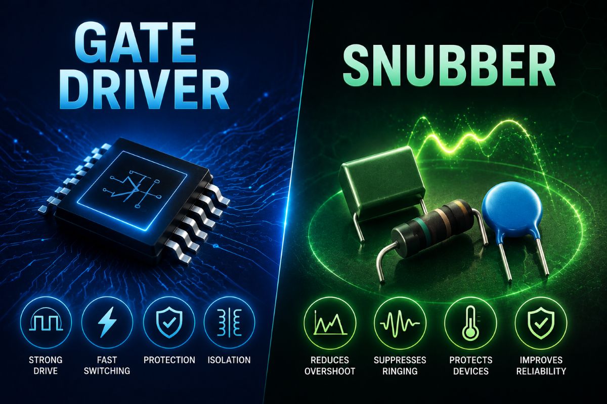
Gate Driver and Snubber Design
Gate Driver and Snubber Design
For power transistors, MOSFETs, and IGBTs in high-power switching circuits.
Why these circuits matter
High-power semiconductor devices switch large voltage and current, so the control circuit must be designed carefully. A gate driver supplies the correct voltage, current, timing, and protection. A snubber circuit protects the device from voltage spikes, ringing, and excessive dv/dt or di/dt during switching.
Gate Driver Basics
The gate driver is the interface between the low-power controller and the power switch. It amplifies the control signal and provides the required gate current or gate voltage. For MOSFETs and IGBTs, the driver must charge and discharge the gate capacitance quickly to reduce switching loss. For power transistors, the driver must supply sufficient base current for the ON state and remove it fast for turn-off.
Key Design Goals
>Fast turn-on and turn-off.
>Low switching loss.
>Correct isolation between the control and power side.
>Protection against overcurrent, overvoltage, and shoot-through.
Device-wise Gate Drive
>Power transistor: A current-driven base drive is required, so the driver must provide base current and remove stored charge quickly.
>MOSFET: Voltage-driven gate, high input impedance, but the driver must charge the gate capacitance rapidly.
>IGBT: Voltage-driven like MOSFET, but usually needs stronger gate drive and careful turn-off control because of tail current.
Practical Gate Driver Points
>Use an isolated driver for high-side or floating devices.
>Choose a proper gate resistor to control switching speed and reduce ringing.
>Keep gate loop short and low-inductance.
>Use gate-to-source or gate-to-emitter protection if needed.
>Add desaturation or overcurrent protection for IGBTs.
Gate Driver Topologies
>Direct low-side driver.
>Transformer-isolated driver.
>Optocoupler-based isolated driver.
>Dedicated gate-driver IC with bootstrap supply.
Snubber Circuit Purpose
A snubber circuit limits voltage spikes, suppresses oscillation, and protects the switch/semiconductor device during turn-on and turn-off. It also helps reduce electromagnetic interference and keeps the device’s operation inside the safe operating area.
Common Snubber Types
>RC snubber: Used across the switch to reduce dv/dt and ringing.
>RCD snubber: Better for absorbing inductive energy in switching converters.
>C snubber: Simple capacitor-only protection for surge reduction.
>Clamp circuits: Used to limit peak voltage during switching transients.
RC Snubber Design Idea
Place the capacitor and resistor in series across the device or across the load path, depending on the circuit. The capacitor absorbs a fast voltage rise, while the resistor damps oscillation and dissipates stored energy. This is widely used with MOSFETs and IGBTs in inductive loads.
Design Checklist
>Know device ratings for voltage, current, and switching speed.
>Estimate stray inductance in wiring and PCB tracks.
>Set gate resistance to balance speed and EMI.
>Verify thermal loss in the snubber resistor.
>Test waveform overshoot and ringing on oscilloscope.
Final Summary
A good gate driver makes the power device switch faster, safer, and with lower loss. A good snubber protects the device from destructive transient stress. In high-power circuits, both are not optional extra; they are essential parts of a reliable design.