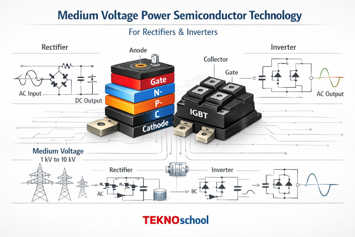
Medium Voltage Power Semiconductor Technology
Medium Voltage Power Semiconductor Technology for Rectifiers and Inverters
The choice of power semiconductor technology dictates the architecture of the input-side rectifier (AC to DC conversion) and the output-side inverter (DC to AC conversion). Over the last three decades, this domain has evolved from line-commutated, high-loss architectures to high-frequency, fully controlled topologies. This deep-dive technical article analyzes the leading semiconductor devices, compares their applications in rectifiers and inverters, explores circuit configurations, and highlights the disruptive impact of Wide Bandgap (WBG) materials.
Medium Voltage (MV) power conversion systems—typically operating within the range of 1 kV to 6.9 kV AC line voltage—constitute the backbone of heavy industrial automation, deep-sea marine propulsion, multi-megawatt wind turbines, and utility-scale grid infrastructure. At the core of these massive systems are power semiconductor devices engineered to block several kilovolts while conducting thousands of amperes with minimal conduction and switching losses.
1. Core Semiconductor Devices in Medium Voltage Applications
MV topologies rely on a specialized class of semiconductors. Unlike Low Voltage (LV) systems, where silicon MOSFETs dominate, MV systems must carefully balance high blocking voltage with thermal dissipation limits. The dominant silicon-based devices are analyzed below.
Insulated Gate Bipolar Transistors (IGBTs) & Press-Pack IGBTs
The Silicon IGBT combines the simple gate drive physics of a MOSFET with the high current density and low forward voltage drop of a bipolar transistor. In the MV arena, IGBT modules are rated from 1.7 kV up to 6.5 kV. For high-reliability applications, such as high-voltage direct current (HVDC) transmission or large Medium Voltage Drives (MVDs), Press-Pack IGBTs (PPIs) are utilized. PPIs lack wire bonds; instead, electrical and thermal contacts are maintained via physical mechanical pressure. This eliminates wire-bond liftoff failures and guarantees a predictable short-circuit failure mode, which is essential for establishing series-connected redundancy.
Integrated Gate-Commutated Thyristors (IGCTs)
The IGCT is a hard-driven evolution of the Gate Turn-Off (GTO) thyristor. By integrating a low-inductance multilayer gate drive circuit directly with the semiconductor wafer, the IGCT can transition from the conducting state to the blocking state instantaneously, forcing the device out of latch-up before damage occurs. The IGCT combines the ultra-low conduction losses of a thyristor wafer with the controlled turn-off capability of an IGBT. They are primarily available in voltage ratings from 4.5 kV to 10 kV, making them optimal for the highest power brackets of MVDs and Flexible AC Transmission Systems (FACTS).
Fast Recovery Diodes (FRDs) & Silicon Controlled Rectifiers (SCRs)
For passive or line-commutated conversion, line-frequency Silicon Controlled Rectifiers (Thyristors) and Fast Recovery Diodes remain indispensable. MV rectifiers use high-power SCRs to manage high surge currents (Itsm) and high reverse blocking voltages. When paired with active switching elements in inverters, specialized FRDs with tailored reverse-recovery characteristics (Qrr) are required to minimize freewheeling losses and prevent destructive voltage spikes.
Technical Profile: Device Characterization Breakdown
Silicon IGBT Module
Voltage Range: 1.7 kV – 6.5 kV
Current Range: 100 A – 1200 A
Typical Switching Frequency: 500 Hz – 2,000 Hz
Conduction Loss: Moderate
Primary Applications: Standard MVD Inverters, Wind Turbines
Press-Pack IGBT (PPI)
Voltage Range: 3.3 kV – 4.5 kV
Current Range: 1200 A – 3000 A
Typical Switching Frequency: 500 Hz – 1,500 Hz
Conduction Loss: Moderate
Primary Applications: Marine Propulsion, Pumped Storage, HVDC
Asymmetric IGCT
Voltage Range: 4.5 kV – 6.5 kV
Current Range: 1000 A – 4000 A
Typical Switching Frequency: 200 Hz – 500 Hz
Conduction Loss: Very Low
Primary Applications: High-Power Inverters, STATCOMs
Phase Control Thyristor (SCR)
Voltage Range: 2.1 kV – 8.5 kV
Current Range: 500 A – 6000 A
Typical Switching Frequency: Line Frequency (50/60 Hz)
Conduction Loss: Extremely Low
Primary Applications: LCI Rectifiers, Industrial Smelters
2. Rectifier Technology in Medium Voltage Systems
The rectifier converts incoming three-phase AC utility power into a stable DC-link voltage. In MV systems, minimizing Total Harmonic Distortion (THD) on the grid side and maintaining a high displacement power factor are critical compliance parameters under international standards like IEEE 519.
Line-Commutated Rectifiers (Multipulse Diode/SCR)
The standard industrial approach relies on multipulse topologies—specifically 12-pulse, 18-pulse, or 24-pulse configurations. By using an isolation transformer with multiple phase-shifted secondary windings (e.g., delta-delta and delta-wye for a 12-pulse system), specific low-order harmonics are canceled.
The harmonic order (h) generated on the AC side is defined by:
h = kP ± 1 (where k is an integer and P is the pulse number)
An 18-pulse rectifier effectively eliminates the 5th, 7th, 11th, and 13th harmonics without requiring passive filters. SCR-based multipulse rectifiers allow for soft-charging the DC-link capacitors and regulating the DC bus voltage, though they introduce a lagging power factor when gated at deep firing angles.
Active Front End (AFE) Rectifiers
For applications requiring regenerative braking (such as downhill conveyors, mine hoists, and test benches) or strict unity power factor compliance, Active Front End rectifiers are mandated. An AFE utilizes controlled switches (IGBTs or IGCTs) identical to the inverter side. By implementing Pulse Width Modulation (PWM) or Direct Power Control (DPC), the AFE shapes the incoming AC line current into a clean sinusoid in phase with the voltage, reducing current THD to under 3% while allowing bi-directional power flow back into the grid.
3. Inverter Technology in Medium Voltage Systems
The inverter stage converts the DC-link energy back into variable-frequency, variable-voltage AC power to drive synchronous or induction motors, or inject power into the utility grid. Due to the high DC-link voltage, a single semiconductor device cannot directly span the entire DC bus without exceeding its Safe Operating Area (SOA). This necessitates multi-level topologies.
Design Paradigm: Multi-level topologies synthesize an output voltage waveform from multiple discrete DC voltage steps. This reduces the voltage stress (dv/dt) applied to the motor windings, mitigates bearing currents, and allows the use of lower-rated, higher-efficiency semiconductors.
Neutral-Point Clamped (NPC) Topologies
The Three-Level NPC inverter remains one of the most widely deployed MV topologies. It introduces a central neutral point tap on the DC-link capacitor bank. Fast clamping diodes tie the output phase node to this neutral point, allowing each switching element to experience only half of the total DC-link voltage. This configuration delivers a 3-level phase-to-neutral voltage waveform, significantly improving output harmonic quality compared to standard 2-level alternatives.
Cascaded H-Bridge (CHB) Inverters
For higher voltage levels (6.6 kV and above), the Cascaded H-Bridge architecture dominates. The CHB topology connects multiple low-voltage single-phase H-bridge inverter modules in series per phase. Each H-bridge is fed by an isolated secondary winding from a complex multi-winding phase-shifting transformer. Through carrier-interleaved PWM strategies, the effective switching frequency seen by the motor is the product of the individual module switching frequency and the number of shifted modules. This achieves ultra-low THD outputs, eliminating the need for bulky, expensive sine-wave filters.
Modular Multilevel Converters (MMC)
Predominantly applied in utility-scale grid connections, HVDC transmission, and ultra-high-power industrial drives, the MMC uses series-connected half-bridge or full-bridge submodules, each containing its own DC capacitor. The output voltage waveform is assembled from dozens of tiny voltage steps, approaching a near-perfect sinusoidal profile with negligible switching losses, as individual submodules switch at very low frequencies.
4. Comparative Operational Analysis
To optimize medium voltage system performance, engineers must balance the trade-offs between the input rectifier and output inverter topologies based on system dynamics.
Architectural Breakdown: System Topology Comparisons
18/24-Pulse Passive Rectifier
Semiconductors: Standard Rectifier Diodes
Efficiency: 98.5% – 99.2% (Highest efficiency footprint)
Harmonic Profile: Low Grid THD; inherently compliant with IEEE 519 standards.
Complexity: Low circuit complexity, but requires heavy phase-shifting transformers.
Active Front End (AFE) Rectifier
Semiconductors: MV-IGBTs / IGCTs
Efficiency: 97.0% – 98.2%
Harmonic Profile: Sinusoidal current injection with minor high-frequency switching ripple.
Complexity: High complexity; necessitates bidirectional controls and LCL line filters.
3-Level NPC Inverter
Semiconductors: 3.3 kV or 4.5 kV IGBTs / Fast Recovery Diodes
Efficiency: 97.5% – 98.5%
Harmonic Profile: Moderate voltage stress (dv/dt); occasionally requires minor motor de-rating.
Complexity: Medium complexity; depends on strict neutral-point voltage balancing algorithms.
Cascaded H-Bridge Inverter
Semiconductors: 1.7 kV IGBTs + Integrated Diodes
Efficiency: 96.5% – 98.0%
Harmonic Profile: Excellent output profile; generates a near-perfect sinusoidal wave to the motor.
Complexity: High mechanical and structural complexity due to a high overall component count.
5. The Wide Bandgap (WBG) Revolution in Medium Voltage
While silicon (Si) bipolar devices have reached their empirical physical limits, Silicon Carbide (SiC) technology is revolutionizing the MV power electronics landscape. The critical material properties of SiC—namely a 10x higher critical electric breakdown field and a 3x higher thermal conductivity—fundamentally transform device architecture.
In the MV space, High-Voltage SiC MOSFETs rated at 3.3 kV, 6.5 kV, and even 10 kV are shifting engineering paradigms. Because MOSFETs are unipolar devices, they do not exhibit the minority-carrier storage charge found in IGBTs and IGCTs, which completely eliminates the characteristic “tail current” during turn-off.
This absence of tail current reduces switching losses by up to 80%. Consequently, a 6.5 kV SiC MOSFET can operate smoothly at switching frequencies of 10 kHz to 20 kHz, compared to a maximum of 1 kHz for a silicon counterpart. This drastic increase in switching frequency reduces the volumetric footprint of passive components—such as DC-link capacitors, phase AC reactors, and isolation transformers—by over 50%, paving the way for high-power-density Solid-State Transformers (SSTs) and highly efficient green energy grid interfaces.
6. Conclusion
Medium voltage power semiconductor technology represents a sophisticated trade-off between thermal management, blocking voltage capabilities, and switching efficiency. For extremely high power configurations, the ultra-low conduction loss of the IGCT remains superior. For high-bandwidth dynamic control and standardized industrial topologies, the Silicon IGBT—especially in its press-pack manifestation—remains highly relevant.
Concurrently, the commercial maturation of high-voltage Silicon Carbide power devices is rewriting the efficiency equations, pushing operating frequencies and thermal boundaries toward unprecedented performance levels.